Advanced Technology PCBs
Advanced PCBs come in a number of materials options, with a 0 to 40 layer count and multiple plating finishes. Quantity doesn’t matter; we will make as few as one PCB or as many as 10,000 without ever compromising the quality. All orders for advanced PCBs undergo the same rigorous fabrication and quality-check process — they are inspected to either IPC Class 2 or IPC Class 3 depending on the option chosen.
Specifications | Standard Specs | Custom |
|---|---|---|
Layer Count | 0 - 10 Layers | 0 - 40 Layers |
Turn Time | Same Day - 5 Day | Same Day - 4 Weeks |
Quantity Req. | 1 - 10000+ | 1 - 10000+ |
Materials | FR-4 | FR-4 / Rogers / Polyimide / Aluminum Clad / High-Temp. FR4 / Halogen Free, Mid to Low Loss, High Speed Digital/ RF, Buried Capacitance/ Flex |
Plate Finish | Lead-Free HAL* | Electrolytic Hard Gold / Soft Gold / ENIG / ENIPIG/ OSP-HT/ Nickel / Immersion Silver / Leaded & Lead-Free HAL |
Cert. / Qualifications | IPC Class 2 - A600 | IPC6012 Class 2-3A / IPC6012 Class 3 DS/IPC6018 Class 3 MIL-PRF-31032 / MIL-PRF-55110 / ISO 9001:2008 / AS9100D / MIL-P-50884 Certified ITAR / IPC 6013 Class 3 & 3A/ES/ IPC 1791 Trusted Electronics/ CMMC V2.0 L2/ Others |
Board Thickness | .031" / .062" / .093" / .125" | Full Range Available |
Copper Weight | 1 oz. Inner / Up to 2 oz. Outer | 0.5 - 4 oz. Inner / 1-20 oz. Outer |
Trace / Space | 5 / 5 Mils | Down to 2.75 / 3 Mils |
Standard vs. advanced
Specifications | Standard | Custom |
|---|---|---|
Layer Count | 0 - 10 Layers | 0 - 40 Layers |
Turn Time | Same Day - 5 Day | Same Day - 4 Weeks |
Quantity Req. | 1 - 10000+ | 1 - 10000+ |
Materials | FR-4 | FR-4/Rogers/Polyimide/Aluminum Clad/High-Temp. FR4/Others » |
Plating Finish | Lead-Free HAL* | Electrolytic Hard Gold/Soft Gold/ENIG/Nickel/Immersion Silver OSP/Leaded & Lead-Free HAL |
Cert. / Qualifications | IPC Class 2 - A600 | IPC6012 Class 2-3A / IPC6018 Class 3 MIL-PRF-31032 / MIL-PRF-55110 / ISO 9001:2008 / AS9100C / More » |
Board Thickness | .031" / .062" / .093" / .125" | Full Range Available |
Copper Weight | 1 oz. Inner / Up to 2 oz. Outer | 0.5 - 4 oz. Inner / 1 - 20 oz. Outer |
Trace/Space | 5 / 5 Mils | Down to 2.75 / 3 Mils |
Solder Mask (LPI) | Green | Various Color Options |
Legend | White | Various Color Options |
Min. Hole Size | 0.010" | 0.004" |
Hole Tolerance | +/- 0.005" | +/- 0.003" (Upon Request) |
Rout Tolerance | +/- 0.010" | +/- 0.005" (Upon Request) |
Slots/Cutouts/Edges | Non-Plated Only | Plated / Non-Plated |
Plated Holes | Plated / Non-Plated | Plated / Non-Plated |
UL Markings/Dates | Yes** | Yes** |
Lead-Free Markings | Yes | Yes |
Gold Fingers | Yes | Yes |
Fiducials | Yes | Yes |
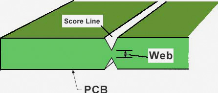
Scoring | Yes | Yes |
ITAR | Yes | Yes |
Castellated Holes | X | Yes |
Controlled Dielectric | X | Yes |
Controlled Impedance | X | Yes |
Counter Sinks | X | Yes |
Counter Bores | X | Yes |
Blind/Buried Vias | X | Yes |
Microvias | X | Yes |
Mask Plugged Vias | X | Yes |
Via-in-Pad | X | Yes |
Etch Back | X | Yes |
Tetra Etch | X | Yes |
Cover Coat | X | Yes |
Cavity Process | X | Yes |
Laser Rout | X | Yes |
LPI Legend | X | Yes |
Edge Mill | X | Yes |
Unique Serialization | X | Yes |
Back Drilling | X | Yes |
Controlled Depth Drill | X | Yes |
* Standard Spec pricing assumes lead-free HAL. Alternatively, board finish may be upgraded to ENIG or Silver at no additional cost in the rare event lead-free HAL becomes temporarily unavailable.
** Added markings contingent on available space on boards. 94V-0 may be added upon request at the time of order entry or if noted in files.
Please Note: Holes will be plated if no specifications provided. Default Solder Mask color is Green unless another color option is requested. Default Legend (Silkscreen) color is White unless another color option is requested.
Still wondering whether or not your board is a Standard or Advanced PCB?
If you are still debating standard vs. advanced PCB, keep in mind what you ultimately need your board to do. When you design your PCBs you can use our free DFM file check system to avoid CAM holds. You can also find a full list of capabilities online to help inform your decision.
AdvancedPCBs: Capabilities
AdvancedPCB manufacturing capabilities meet your unique product demands and design criteria:
- Buried Chip Resistors
- Blind and Buried Vias
- Up to 40 layers
- .00275" Trace/Space
- Air Pockets between layers
- Via-in-Pad
- Cavity Boards
- ITAR Registered
- Stacked Microvias
- Laser Drilled Microvias (HDI)
- Laser Direct Imaging (LDI)
- Down to .3mm Pitch
- Heavy Copper (up to 20 oz.)
- Multilayer RF Designs (up to 8 layers)
- Oversized Boards (up to 37" x 120")
AdvancedPCBs: Certifications
We offer a range of certifications to help you meet your quality standards:
- IPC 6012 Class 3 & 3A/ES
- RoHS
- REACH
- PCB Board UL
- ITAR
- MIL-PRF-31032
- MIL-PRF-55110
- MIL-P-50884
- AS9100D with ISO 9001:2015
- 31032 GI 8-layer
- Awarded IPC 1791 Qualified Manufacturers Listing (QML)
Advanced PCBs: Laminates
Deciding on the right laminate for your PCBs is an important part of the design process. The laminate used on your printed circuit boards will help achieve final thickness and give you a PCB that you can use for your application. At the end of the day, you need your circuit board to connect all of your components and work efficiently in the intended application. When you order your PCBs from AdvancedPCB you can get peace of mind knowing that the finished boards meet the toughest standards set by the industry for quality.
Laminate | Type | Tg Celsius | Td Celsius | T-260 Minutes | T-288 Minutes | Dk | Df | UL94 |
|---|---|---|---|---|---|---|---|---|
Aluminum Clad | @ 1 MHz | @ 1 MHz | ||||||
130 | 380 | 4.8 | 0.016 | V0 | ||||
Isola | @ 1 GHz | @ 1 GHz | ||||||
FR4 / Phenolic | 180 | 340 | 60 | 30 | 4.04 @ 2 GHz | 0.021 @ 2 GHz | V0 | |
FR4 / Phenolic | 180 | 340 | 60 | >15 | 4.01 @ 2 GHz | 0.0200 @ 2 GHz | V0 | |
FR4 | 135 | 10 | 4.34 | 0.016 | V0 | |||
FR4 High Temp | 170 | 300 | 10 | >2 | 3.95 | 0.0161 | V0 | |
FR4 | 190 | 360 | 60 | >30 | 3.69 | 0.0091 | V0 | |
Modified Epoxy | 225 | 364 | 60 | >20 | 3.58 | 0.0059 | V0 | |
Polyimide | 260 | 416 | 60 | 60 | 3.78 | 0.0172 | HB | |
Polyimide | 260 | 396 | 60 | 60 | 3.78 | 0.0172 | V0 | |
Nelco | 1 GHz | 2.5 GHz | ||||||
FR4 High Temp | 175 | 325 | 4-8 | 4.0 @ 2.5 GHz | 0.022 | V0 | ||
Modified Epoxy | 175 | 345 | 30 | 4.1 | 0.02 | V0 | ||
Modified Epoxy | 190 | 350 | >60 | 3.7 | 0.008 | V0 | ||
Modified Epoxy | 210 - 240 | 350 | >30 | >10 | 3.7 | 0.009 | V0 | |
N4000-6 SI/EP | Modified Epoxy | 210 - 240 | 350 | >30 | >10 | 3.7 | 0.009 | V0 |
FR4 High Temp | 175 - 185 | 350 | >60 | 15 | 4.3 | 0.015 | V0 | |
Arlon | 1 MHz | 1 MHz | ||||||
Cer/Glass | 250 | 407 | >60 | >60 | 4.2 | 0.01 | HB | |
Rogers | 8-40 GHz | 10 GHz | ||||||
PTFE / Glass | 500 | 2.2 | 0.0009 | V0 | ||||
PTFE / Microfiber | 500 | 2.33 | 0.0012 | V0 | ||||
Cer/PTFE | 500 | 2.94 | 0.0012 | V0 | ||||
Cer/PTFE | 500 | 6.45 | 0.0027 @ 10 GHz/A | V0 | ||||
Cer/PTFE | 500 | 10.7 | 0.0023 @ 10 GHz/A | V0 | ||||
Cer/PTFE | 500 | 3 | 0.001 | V0 | ||||
Cer/PTFE | 500 | 6.5 | 0.002 | V0 | ||||
Cer/PTFE | 500 | 11.2 | 0.0022 | V0 | ||||
Cer/PTFE | 500 | 3.02 | 0.0016 | V0 | ||||
Cer/PTFE | 500 | 10.8 | 0.0027 | V0 | ||||
Hydrocarbon/Cer | >280 | 425 | 3.55 | 0.0027 | N/A | |||
Hydrocarbon/Cer | >280 | 390 | 3.66 | 0.0037 | V0 | |||
Hydrocarbon/Cer | >280 | 390 | 3.3 ± 0.05 @ 10 GHz | 0.004 | V0 | |||
Taconic | 10 GHz | 10 GHz | ||||||
PTFE / Glass | 3.2 | 0.003 | V0 | |||||
PTFE / Glass | 2.95 | 0.0028 | V0 | |||||
PTFE / Glass | 2.5 @ 1 MHz | 0.0006 @ 1 MHz | V0 | |||||
PTFE / Glass | 553 | 2.55 | 0.0012 @ 1.9 GHz | V0 |
Advanced PCBs: Multi-layer stackups
For these or any specific stackup that you require, be sure to order as "Custom" and select "Controlled Dielectric". You may select ½, 1 or 2 ounce inner layer copper foil for your printed circuit board.
Calculate the thickness of your custom stackup.
The chart that we link to below provides the thickness for a single ply (sheet) of each style of Pre-Preg after processing. These are grouped by the weight and type of the internal conductor layer (typical signal and plane layers) that they will be adjacent to (columns A-F). Those that are adjacent to the top and bottom copper layers will use the column designated for these (column G) regardless of the layer type. All plies that are not directly against a conductor layer (use for situations with more than 2 plies in an opening) will use the additional plies values (column H). These values are based on a minimum of 2 plies of pre-preg per opening between foil and cores or between cores.
Thickness guide (mils, 1/1000 inch)*,** | ||||||||
|---|---|---|---|---|---|---|---|---|
A | B | C | D | E | F | G | H | |
Pre-Preg Styles | Against core with .5 oz copper and signal traces utilizing 30% of the board area | Against core with .5 oz copper and signal traces utilizing 70% of the board area | Against core with 1 oz copper and signal traces utilizing 30% of the board area | Against core with 1 oz copper and signal traces utilizing 70% of the board area | Against core with 2 oz copper and signal traces utilizing 30% of the board area | Against core with 2 oz copper and signal traces utilizing 70% of the board area | Against the top and bottom copper layers (foil) | Additional plies that are not directly against conductor layers |
106 | 1.9 | 2.2 | 1.5 | 2.0 | 0.5 | 1.5 | 2.3 | 2.1 |
1080 | 2.6 | 2.8 | 2.1 | 2.6 | 1.1 | 2.2 | 3.0 | 2.7 |
2113 | 3.5 | 3.7 | 3.0 | 3.5 | 2.0 | 3.1 | 3.9 | 3.5 |
2116 | 4.7 | 4.9 | 4.2 | 4.7 | 3.2 | 4.3 | 5.1 | 4.6 |
7628 | 6.5 | 6.8 | 6.0 | 6.5 | 5.0 | 6.1 | 6.9 | 6.2 |
*This thickness guide is provided as a guide only. The actual thickness will be affected by the copper distribution within the design as well as within the production panels
**The dielectric thickness requirements supplied with an order will be interpreted with a minimum, 10% tolerance.
Example:
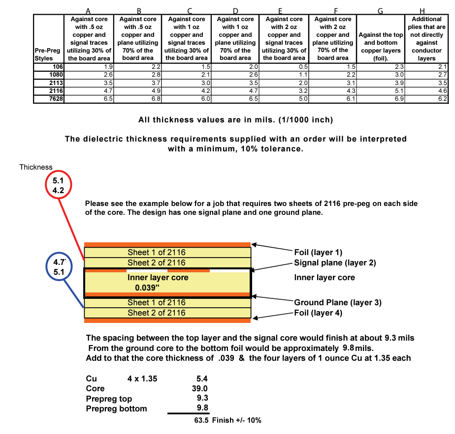
| Layer | Layer Description | Thickness |
|---|---|---|
| Layer 1 | Foil: 1 oz foil thickness 0.00135” | 0.00135” |
| Prepreg top | Sheet 1 of Prepreg style 2116 (Column G, Row 2116: 5.1 mils) | 0.0051” |
| Prepreg top | Sheet 2 of Prepreg style 2116 (Column C, Row 2116: 4.2 mils) | 0.0042” |
| Layer 2 | Signal Plane: 1 oz foil thickness 0.00135” | 0.00135” |
| Core | Laminate core 0.039” | 0.039” |
| Layer 3 | Ground Plane: 1 oz foil thickness 0.00135” | 0.00135” |
Prepreg bottom | Sheet 1 of Prepreg style 2116 (Column D, Row 2116: 4.7 mils) | 0.0047” |
| Prepreg bottom | Sheet 2 of Prepreg style 2116 (Column G, Row 2116: 5.1 mils) | 0.0051” |
| Layer 4 | Foil: 1 oz foil thickness 0.00135” | 0.00135” |
| Total thickness (Finish +/- 10%) | 0.0635” | |
See the following table for the final thickness options of our multilayer boards:
0.020" | 0.031" | 0.040" | 0.047" | 0.062" | 0.093" | 0.125" | Max Board Size | |
|---|---|---|---|---|---|---|---|---|
4-layer | ✔ | ✔ | ✔ | ✔ | ✔ | ✔ | ✔ | 16” x 22” |
6-layer | X | ✔ | ✔ | ✔ | ✔ | ✔ | ✔ | 16” x 22” |
8-layer | X | X | X | X | ✔ | ✔ | ✔ | 16” x 22” |
10-layer | X | X | X | X | ✔ | ✔ | ✔ | 14” x 20” |
11-layer and up | X | X | X | X | ✔ | ✔ | ✔ | >14” x 20” |
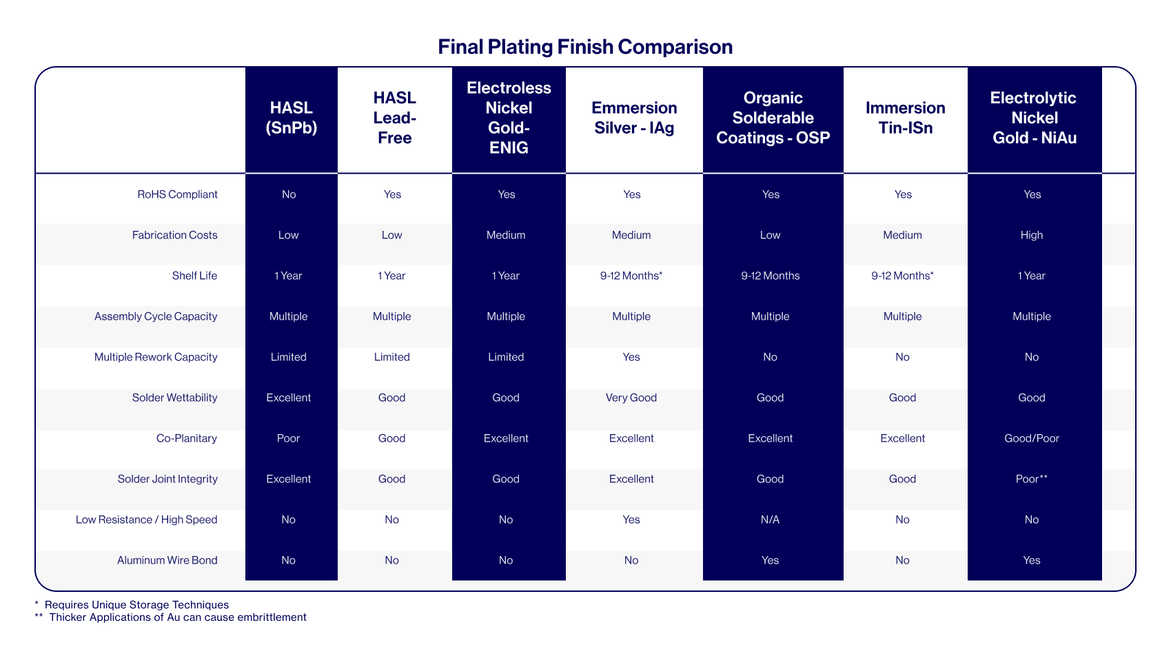
Advanced PCBs: Board Finishes
It’s important to have the PCBs finished so their materials will not decay and so there is a consistent surface for connecting components to the board. We can provide you with UL-approved circuit boards with a tin copper alloy lead-free solder finish that meets the requirements of RoHS, REACH and Conflict Metals regulations. See the list of available board finishes for Advanced PCBs.
Electrical Test
We use two types of testing equipment on your circuit boards:
- Fixtureless: Flying probe with Everett Charles ATG test machines
- Fixture-based: Universal grid testing
 Flying probe testing
  Universal grid testing