


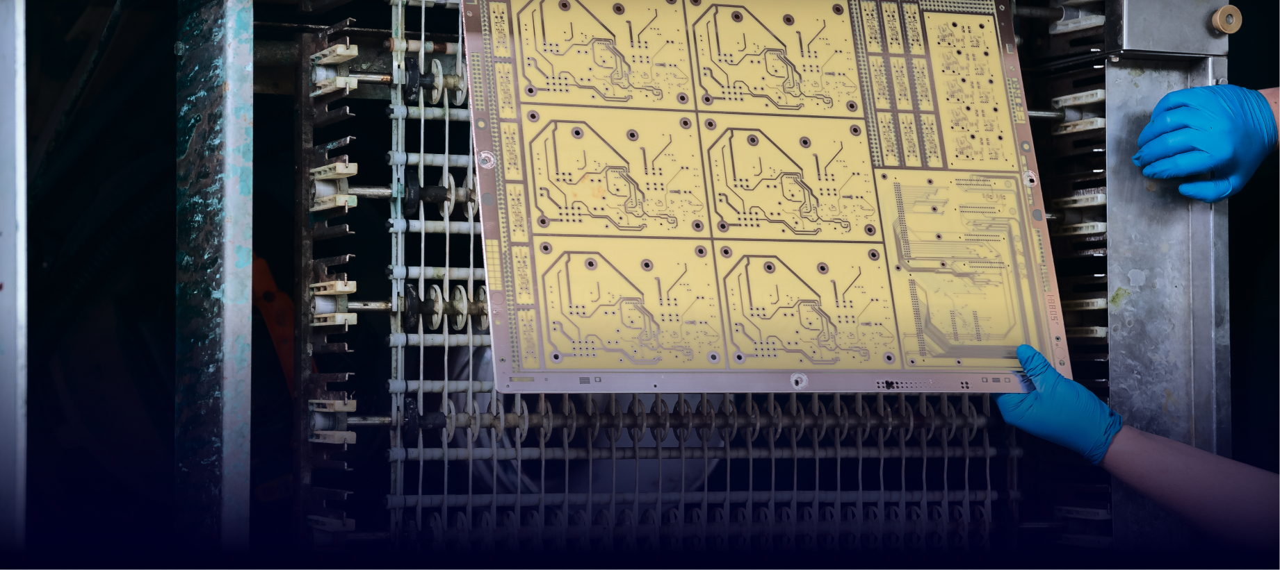
2-Layer vs. 4-Layer Printed Circuit Boards

When it comes to printed circuit boards (PCBs), there are infinite possibilities for how many layers you can have. Some supercomputers have nearly a hundred layers in their construction, but, the most common layered PCBs usually have only two or four layers. Read on to find out what the differences are and how you can make an informed decision for your next project.
2-Layer PCBs
Compared to 4-layer PCBs, 2-layer PCBs are much easier to work with due to their simple design. While not as simple as 1-layer PCBs, they’re as straightforward as you can get without sacrificing the functionality of double-sided inputs. The reduced complexity leads to an equally reduced price tag, but this means there are fewer possibilities than with the 4-layer PCB. As a pro, though, there is no propagation delay with the signal.
4-Layer PCBs
4-layer PCBs have much greater surface area than a 2-layer PCB, increasing the possibilities. As a result, they can be great for more complex devices. Because of their complexity, the production cost will be higher and development will be a bit slower. They are also more likely to have propagation delays, so be sure to factor in extra production time to any project timeline.
What are the Layers Used For?
The most important layer in a PCB is the copper signal layer, which is what the PCBs are named after. While 2-layer PCBs have two signal layers, 4-layer PCBs have – you guessed it – four. These signal layers are used to connect to other electronic components in the device. In between those layers is the insulation layer or core, which is added in between the signal layers to give it structure. In 4-layer PCBs, here’s also the solder mask layer, which is applied on top of the signal layers. This prevents the copper traces from interfering with other metal components on the PCB. They also have a silkscreen layer which is used to add numbers to the different components, making them easier to understand.
If you’re looking for PCB solutions, look no further than AdvancedPCB. We offer PCB assembly, barebones PCBs, free PCB design software, and so much more. Our 24-hour tech support team would love to help you– contact us today.

AdvancedPCB
Related Posts
Vias, Sequential Lamination, and Plating: Navigating Their Role in Signal Integrity for PCB Design
Future trends of the circuit board
