Ask Our Engineers
Posted
10/22/2024

Question:
What happens if I don’t use a solder mask on my PCB?
Answer:
When No Solder Mask is Used in PCB Manufacturing
A critical part of PCB manufacturing, solder masks protect copper traces and prevent unintended solder bridges during assembly. Despite their importance, solder masks might be intentionally omitted in some situations. Let’s look at some specific cases in which manufacturers might forgo a solder mask.
- High-frequency circuits
High-frequency circuits, such as high-speed digital designs and boards that operate in the RF/microwave frequencies up to the millimeter-wave spectrum, are generally more susceptible to parasitics, including stray capacitance between neighboring traces or between traces and ground planes. Board designers must carefully consider avenues that could cause issues with power integrity (PI), signal integrity (SI), and electromagnetic interference (EMI). A potential source of these problems is parasitic capacitance, in which engineers must carefully consider the spacing between conductors as well as the dielectric between them. Any unintended changes in these relationships could impact the behavior of the design and, ultimately, degrade performance. It is not unusual for many of these circuits to forgo solder masks because they often add undesired parasitic capacitance.
This is especially true for RF circuits, in which the high-frequency signal is carried on the outer layer of the board, such as microstrips and grounded coplanar waveguides. As Figure 1 shows, for these types of designs, certain areas—or even the entire board—may be left without a solder mask to reduce interference and ensure optimal signal quality.
.jpg) Figure 1: A low-noise block (LNB) downconverter board with solder mask used in parts of the board, while high-frequency circuits are without a solder mask. Source: Wikimedia Commons
Figure 1: A low-noise block (LNB) downconverter board with solder mask used in parts of the board, while high-frequency circuits are without a solder mask. Source: Wikimedia Commons
- Edge Connector Areas
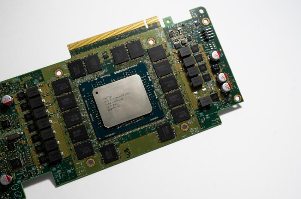
Edge connectors, also known as card-edge connectors, are a common feature in many PCBs, embedding a connector within the PCB to allow it to make electrical contact with external devices or systems. This is often found with motherboards and GPUs for computers (Figure 2) as well as other electronic systems. These connectors, which are often plated with gold for durability and superior conductivity, are also known as gold fingers, with contacts on the top and bottom of the PCB. These are generally made without a solder mask. By leaving these areas exposed, manufacturers ensure reliable connections and consistent performance.
 Figure 2: Gold fingers found on an Intel processor board. Source: Wikimedia commons
- Prototyping and testing
A solder mask adds a thin layer of polymer to protect a finished board from unwanted shorting between conductors (e.g., solder bridges between closely spaced pads), as well as environmental damage and accelerated aging leading to oxidation. However, this has a downside: It prevents access to the PCB’s traces. A solder mask covers everything outside of solder pads and holes/vias. In the early stages of development, the ease of access to the PCB’s copper traces is essential for testing, rework, and debugging. During prototyping, specific regions of the board might be left without a solder mask to facilitate quick testing and modifications. This allows engineers to easily probe or solder components as they refine the design.
- Cost considerations
Sometimes, omitting the solder mask can be a way to reduce manufacturing expenses, especially with low-cost, disposable products such as e-cigarettes, print cartridges, single-use medical devices (e.g., digital pregnancy tests), asset trackers, and even cheap consumer children’s toys. For products that don’t require long-term durability or protection for the copper traces, this can be a viable option.
- Thermal Management
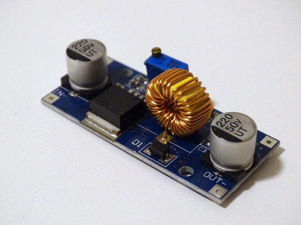
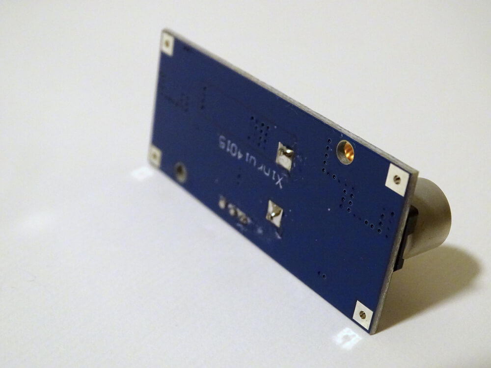
PCBs that deal with high-power components often require careful thermal management, in which components with a high thermal conductivity are used to spread and dissipate heat. This logic can be seen in heatsinks, where the metallic fins increase the amount of surface area that radiates heat from the power device. A solder mask is an insulating material that impedes the spread and distribution of heat, potentially causing components to run too hot and possibly fail. In such designs, exposing bare copper can be beneficial for heat dissipation. By skipping the solder mask in these areas, heat can be more effectively transferred away from the board and into heat sinks or thermal vias, preventing overheating and improving performance. Similar to heat pipes, thermal vias are basically holes located under a surface-mount heat source to transfer heat from one side of the PCB to either the center of the board or to the other side of the board (Figure 3).
Figure 3: The top side (left) and underside (right) of a PCB with components that run hot. The thermal vias can be seen as the small, carefully placed black dots scattered throughout the underside of the board..jpg)

- Aesthetic purposes
In addition, some custom PCB designs, particularly in artistic or niche applications, may intentionally expose copper traces for aesthetic or mechanical purposes. These designs can be found in custom electronics projects, art installations, or other niche applications where the exposed metal serves a functional or decorative role.
Though the solder mask is essential for most PCB designs, sometimes omitting it makes sense. This can be done for engineering purposes, such as ensuring high-frequency performance, mitigating SI/PI issues, or for more optimal thermal design. Other reasons can be more basic, such as cost-saving measures or for aesthetic purposes. All of these specific cases highlight the flexibility and variety in PCB manufacturing.
Browse
All Categories
Recent Posts
View Recent Posts


