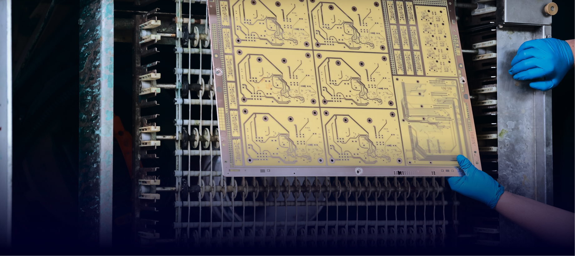
Free Resources and Tools Make Circuit Board Design Easy and Error-Free

Circuit board design is essential in the modern manufacturing process as almost every electronic device uses a PCB (with or without surface-mount technology). And yet, the process of making a PCB is rarely thought of as fast, easy, or without some risks, delays, and errors. If it were just a matter of circuit board design, it would be one thing, but there are many different steps to PCB design.
For instance, there is the initial circuit board design process. Then there are processes like film creation, mapping of copper paths, and V-scoring and testing. This is why promises of same-day production or turnaround are greeted with skepticism and raised eyebrows. However, AdvancedPCB is able to deliver on same-day turnaround times, flawless design, and more.
This is something AdvancedPCB understands. We add value to customers’ experiences and outcomes with such services and benefits as:
Not everything has to be outsourced or complex, and your circuit board design and production don’t have to involve multiple companies that put you at risk for error. When there are such easy, free, and comprehensive solutions, the risks are erased, money and time are saved, and production schedules guaranteed.
Partnering with AdvancedPCB means designers and producers get a unique experience marked by attention to detail. This is different from the “no-touch” approach that so many circuit board design firms are forced to work with. Demanding pre-tested files, they just run the project “as is,” jeopardizing the budget should there be undetected errors. The team at AdvancedPCB runs each circuit board design through expert examinations long before production begins.
Printed circuit board design does not have to be a gamble or a process that involves all kinds of back and forth between designers and producers. Whether you want a one-off or prototype with a fast turnaround time (even a single day), or you are looking for a solution that integrates design, testing, production, and assembly in one space, you’ll find it here at AdvancedPCB.
For instance, there is the initial circuit board design process. Then there are processes like film creation, mapping of copper paths, and V-scoring and testing. This is why promises of same-day production or turnaround are greeted with skepticism and raised eyebrows. However, AdvancedPCB is able to deliver on same-day turnaround times, flawless design, and more.
Single-Space Circuit Board Design and Production Plant
It is rare to find circuit board design solutions in a single facility or space. However, AdvancedPCB has over 25 years in the circuit boards industry and ranks as one of the largest one-stop providers. Specializing in circuit boards and prototypes, we have a comprehensive set of services and solutions that include:- One day PCB production: Among the only PCB providers capable of manufacturing and assembling circuit boards in a single day, we have the ability to provide circuit board designs of great complexity in a short amount of time.
- Full support: Unlike many other manufacturers, our team works with you every step of the way. We begin with a quote based on initial design spec uploads and guide you through to the final production and assembly phases.
- Quality: With free design and testing resources, clients can be assured of the overall quality of the product they will receive. However, a full CAM review is done before any manufacturing begins, as well as visual inspections of the final circuit boards.
- Transparent pricing: There are no hidden fees or sneaky pricing that covers essential services, including stenciling fees, setup fees, and other unnecessary charges.
- One-stop solution: Circuit board design benefits immensely from seamless design, review, and production options. With everything happening under one roof, it means designers and engineers are on-site to evaluate and remediate when necessary. It means no risk for errors, delays, and costly problems.
After Circuit Board Design Comes Evaluation and Production
Of course, circuit board design is not all about production. Yes, speed and efficiency are amazingly beneficial, but only if the initial circuit board design is all it is meant to be.This is something AdvancedPCB understands. We add value to customers’ experiences and outcomes with such services and benefits as:
- No minimum orders: No need to lock a huge segment of the budget into meeting the financial demands of minimum orders on simple to complex circuit board designs with this substantial option.
- CAM engineer evaluations: All products are evaluated by one of our in-house engineers long before production begins in order to spare clients any costly mistakes.
- Free design software: The cost of PCB design software is part of doing business. AdvancedPCB offers proprietary and exclusive PCB Artist software available in an unrestricted format and entirely for free. It downloads to a client’s Windows-based desktop and is capable of up to 28 layers in a single design. The program has over 500k parts from which to choose, integrates a controlled auto-router function to speed up design processes, and offers multi-page schematics for more complex projects. With a complete library of tutorials to train those using the program, there is no reason not to take advantage of it.
- Free evaluation software: For those already using a CAM program of their own, the option for FreeDFM allows the manufacturing quality of a design to be tested. The files are exported in a Gerber format and loaded to the online software, which reviews the entire file, corrects any glitches, and generates a report indicating changes or potential problems.
- Full tech support: While it’s great to have customer support around the clock, few PCB firms offer their clients an opportunity to troubleshoot with the help of a CAM engineer. AdvancedPCB has experts of this kind available 24 hours a day.
Going Above and Beyond for Your Success
Another benefit of working with AdvancedPCB is that it is possible to use our available resources and then order through the free software. Rather than downloading and re-uploading, it is possible to simply use the software options and then run an order through at the end of the review and correction process. The CAM engineer review is always done, regardless of the channel used to order, and there is always a discount for making an order directly through the free resources.Not everything has to be outsourced or complex, and your circuit board design and production don’t have to involve multiple companies that put you at risk for error. When there are such easy, free, and comprehensive solutions, the risks are erased, money and time are saved, and production schedules guaranteed.
Partnering with AdvancedPCB means designers and producers get a unique experience marked by attention to detail. This is different from the “no-touch” approach that so many circuit board design firms are forced to work with. Demanding pre-tested files, they just run the project “as is,” jeopardizing the budget should there be undetected errors. The team at AdvancedPCB runs each circuit board design through expert examinations long before production begins.
Your One-Stop-Shop for PCB Design Needs
Why work with a broker when there is an option to pair up with one-stop specialists? We offer some of the fastest turnaround times and the best on-time shipping record in the industry.Printed circuit board design does not have to be a gamble or a process that involves all kinds of back and forth between designers and producers. Whether you want a one-off or prototype with a fast turnaround time (even a single day), or you are looking for a solution that integrates design, testing, production, and assembly in one space, you’ll find it here at AdvancedPCB.

AdvancedPCB
Related Posts

Vias, Sequential Lamination, and Plating: Navigating Their Role in Signal Integrity for PCB Design
Welcome to the fascinating world of PCB design, where the interplay of various elements shapes the heart of modern electronics. Today, let’s have a chat about something crucial but often underrated – the impact of vias, sequential lamination, and plating on signal integrity.
Vias, Sequential Lamination, and Plating: Navigating Their Role in Signal Integrity for PCB Design
Read More

Future trends of the circuit board
As consumer demands for faster, smaller and more efficient devices intensify, so do printed circuit board requirements. PCBs are the backbone of all electronic devices. They affect their size, speed and functionality.
Future trends of the circuit board
Read More

2-Layer vs. 4-Layer Printed Circuit Boards
When it comes to printed circuit boards (PCBs), there are infinite possibilities for how many layers you can have. Some supercomputers have nearly a hundred layers in their construction, but, the most common layered PCBs usually have only two or four layers.
2-Layer vs. 4-Layer Printed Circuit Boards
Read More
Browse
All Categories
Recent Posts
View Recent Posts


