


How to Better Plan Your Printed Circuit Build

Are you wondering what the easiest and most cost-effective way to build a printed circuit board (PCB), also called a printed wiring board (PWB), is? How do you start? Does AdvancedPCB have any PCB solutions?
Start with a Schematic
A schematic uses symbols to designate the components and shows the components used and how they connect in the circuit and is needed to design the PCB.
PCB Design
The PCB designer uses the schematic and specifications of the components to design the PCB manually or with a computer-aided design (CAD) program like the one offered free through AdvancedPCB.
TIP: To make your PCB look professional:
- Place the components on a 0.10 grid, horizontally (x-axis) or vertically (y-axis), not on angles.
- Place the components with polarity (anodes) facing the same direction in both axes.
The same with resistor stripes.
Inserting the Components on the PCB
The components are inserted manually or by a machine called an automatic insertion machine. This procedure is called PCB electromechanical assembly.
The component wire leads are soldered in place by hand or a wave solder. Some companies bend the wire leads on the solder side of the PCB to hold the components in place before soldering.
Before the Production Run
The making of a prototyping board before the production run is not only a common but wise procedure. By doing so, any errors in the circuitry or printed circuit board design are more likely to be detected.
TIP: Prototype PCBs often lack a solder mask. Make sure the traces are wide enough to handle the amperage with a solder mask.
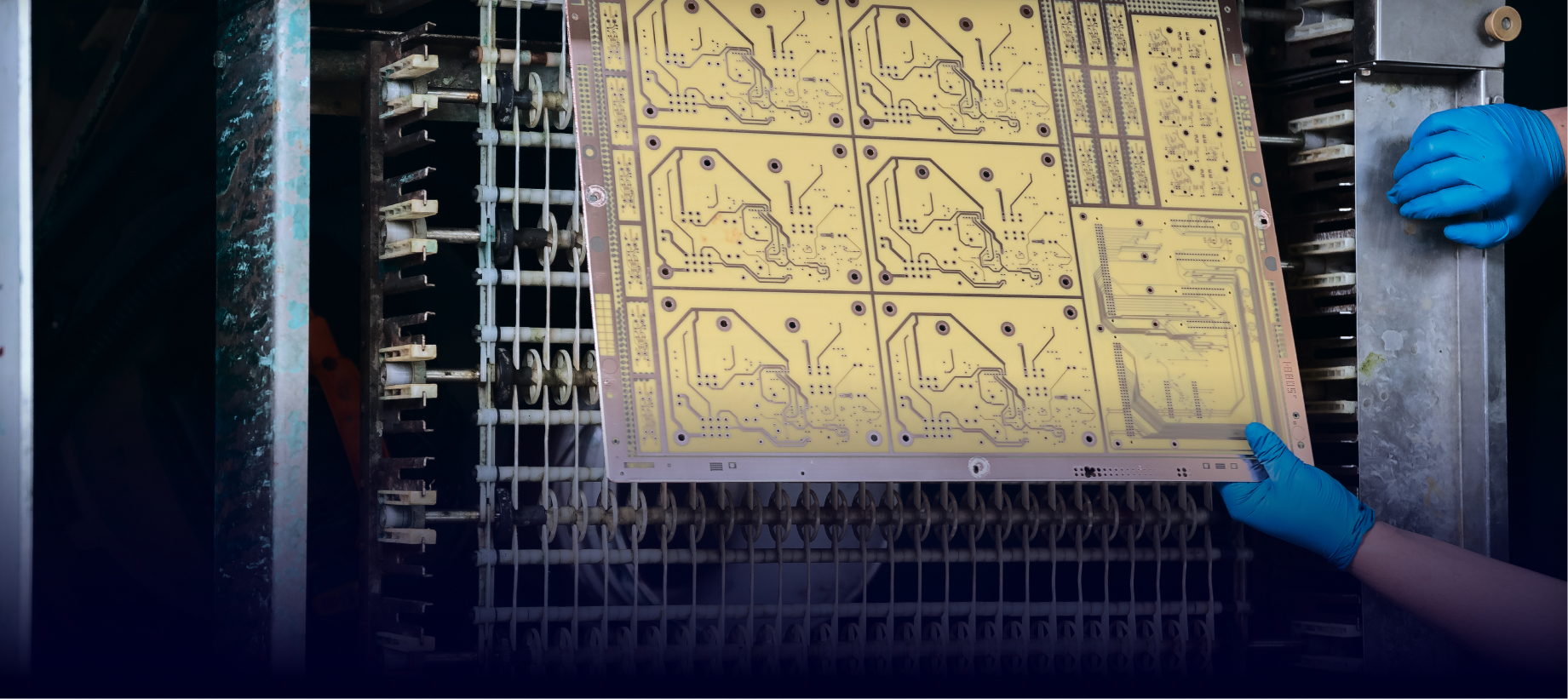
AdvancedPCB Can Solve Your PCB Needs
If you are looking for a one-stop shop for your PCB needs, AdvancedPCB is your PCB solution. From the design of your PCB to making your boards to assembly.
Some of the services provided are:
- PCB Design Layout software
- Free PCB file checks
- Barebones PCBs
- PCB full spec prototyping
- PCB full spec production
- PCB assembly
- PCB stencils
- 0-10 layers PCB (standard)
- 0-40 layers PCB (custom)
- No minimum order
- DOD contracts ready
- Space & flight approved PCB supplier
AdvancedPCB is your market industry expert, whether you are a student, hobbyist, or a manufacturer of defense, aerospace, or medical equipment.
Contact us today for more information or to have a live chat with an expert.

AdvancedPCB
Related Posts
Vias, Sequential Lamination, and Plating: Navigating Their Role in Signal Integrity for PCB Design
Future trends of the circuit board
