Overcoming Common Pitfalls in High-Frequency PCB Design
.jpg?resizemode=force&maxsidesize=500)
High frequency (HF) and radio frequency (RF) are fundamental in multiple domains, such as aerospace, defense, and medicine, and are often encountered in communication systems, radar devices, and imaging equipment. However, the high frequencies usually involve challenges that PCB designers would not typically face in non-HF designs, such as the need for impedance matching, the skin effect, crosstalk, EMI issues, and reflections.
Characteristics of High-Frequency Designs
HF circuits are not characterized by the highest clock frequency in the design; rather, the high-speed signal’s rise time determines whether a circuit qualifies as an HF circuit. Rise times below 5ns are typically common in HF circuits. Faster digital signals have a shorter rise time and, thus, a higher bandwidth in the frequency domain.
In HF designs, passive components are used for impedance matching, filtering, tuning, and signal coupling. They shape the characteristics of the signal without amplifying it. On the contrary, active components are used for signal amplification, modulation, demodulation, and frequency conversion. They play a crucial role in signal strength enhancement and processing.
The Skin Effect and Problems of Transmission Lines in HF Designs
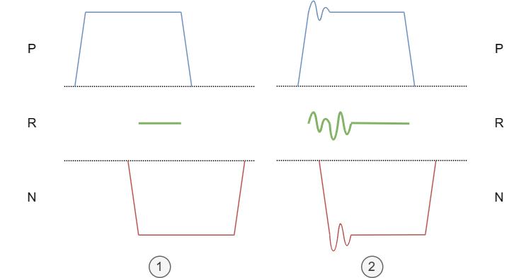
Transmission lines transfer RF signals over long stretches between HF components on a board, ideally maintaining signal integrity and minimizing distortion and crosstalk between adjacent traces. In RF designs, transmission lines often require length-matching, and traces must be designed to have a particular impedance, depending on the target application. Designing transmission lines with a specific impedance helps mitigate signal reflections, standing waves, signal deterioration, and EMI problems.
A perfect conductor would have no capacitive losses or other side effects, such as the skin effect. However, copper is not an ideal conductor; therefore, considering the skin effect is critical in HF designs. Skin effect losses in transmission lines increase with the transmitted signal’s frequency. The problem can be summarized as the appearance of electric fields that concentrate along the edges of an HF transmission line. At very high frequencies, the field does not have enough time to spread throughout the entire conductive surface. Thus, the current is concentrated on a part of the copper surface, not the whole trace. The higher the frequency, the narrower the area becomes.
This energy is expressed as a magnetic field that spreads in all directions around the entire trace, not just in the direction of the next reference plane. This phenomenon is especially problematic in microstrip traces, as one side of the trace does not have a clear low-impedance return path to a reference. In those cases, the signal could induce inductive crosstalk in nearby transmission lines if not accounted for.

PCB designers employ various methods to combat these problems. First, changing the stack up so that critical HF transmission lines are manufactured as strip lines with distinct reference planes on either side helps reduce skin effect losses while simultaneously containing EMI noise. However, traces that are short enough not to act as distributed transmission lines would not benefit from this measure due to additional via losses.
Distributing current over larger copper areas can also help mitigate skin effect losses. Engineers can choose to widen traces or increase their thickness as long as the changes are in accordance with the trace’s target impedance. Increasing trace width further reduces trace inductance and helps reduce inductive crosstalk between transmission lines. Similarly, designers can choose smoother types of copper, because copper roughness highly influences skin effect losses, especially at very high frequencies. Additionally, changing the board substrate changes the dielectric constant, which thus also influences skin effect losses.
Length Matching in HF Designs
Besides designing traces for a specific target impedance, length matching is a critical tool to ensure the reliability and correctness of high-frequency designs. Matching trace lengths serves two purposes. In matched-pair digital signals, the out-of-sync arrival of one line’s signal compared to the other can cause digital states to be too short for the receiving end to decode, leading to incorrect data transmission. Second, noise originating from the sending end could cancel out if induced simultaneously on both lines of a differential pair. However, if the noise signals are not synchronized, they don’t cancel out and exacerbate the noise pattern in the worst case.

Thus, adding length-matching structures to the shorter lines ensures that the trace lengths and, more importantly, the signal transmission times are nearly identical. Designers can choose from various patterns as long as the added structures are symmetrical. However, serpentine routing and trombone length matching are among the most popular. When matching multiple groups of length-matched pairs, both traces in all shorter groups should be extended to match the longest group. If applicable, designers should add the length-matching structures closer to the transmitting end rather than the receiver, to ensure that signals travel synchronously over a more considerable distance to prevent them from drifting apart as they propagate along a trace.
Finally, keep high-frequency lines on a PCB as far apart as possible and sensible. Traces should be separated by at least three times the shortest distance of an involved transmission line to its next suitable reference plane.
The Role of Via Stubs in HF Designs
Vias play a crucial role in HF designs, and engineers should pay due diligence to the same aspects as in regular PCBs regarding signal integrity and low-impedance return paths. In that sense, adding ground vias next to signal vias helps to provide deterministic low-impedance return paths for signals when traversing layers.
Additionally, via stubs require more careful handling, because they can act as small unterminated transmission lines and result in impedance mismatches and signal reflections when not accounted for in an HF design. Analog signals and the different wavelength components of digital signals interact with the via stub. They can get distorted, potentially making the receiver unable to read the original signal.

In those instances, designers should aim to reduce the via stub length to meet their design’s frequency requirements. However, as the ideal target length may not be manufacturable, backdrilling may be necessary to remove leftover stubs.
Ideally, designers want to avoid vias in high-frequency transmission lines by grouping logically related components and keeping connections between them short. However, if transmission line vias are needed, use smaller vias to reduce inductance.
Via Stitching and Via Fences
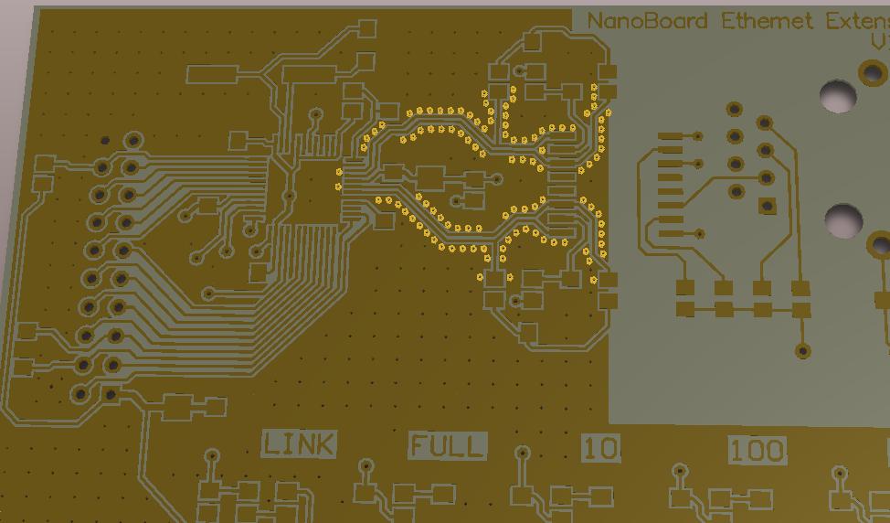
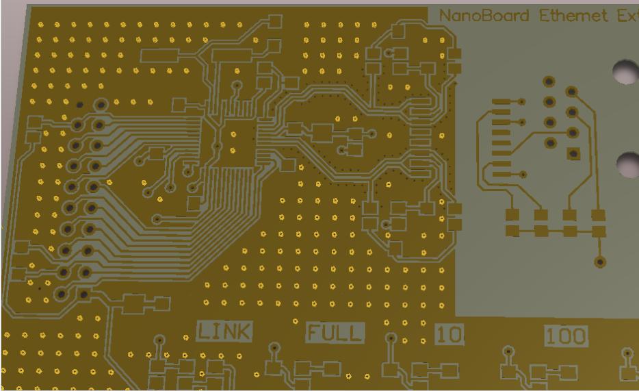
Via fences strategically placed around sensitive components or susceptible functional groups can shield them from EMI by creating a conductive barrier. These via fences are connected to reference planes and provide a low-impedance return path.

Via stitching is a similar technique that tries to connect the same reference plane over multiple layers in the PCB stackup. This technique is particularly effective in minimizing ground loops and reducing noise in HF circuits. If additional impedance control is needed when transitioning between layers, designers can employ tapered vias that offer gradual diameter reduction to help minimize impedance changes and signal reflections.

Summary
High-frequency (HF) and radio-frequency (RF) technologies are pivotal across industries that include aerospace, defense, and medicine. They power essential systems, such as communication networks, radar devices, and medical imaging equipment. Designing PCBs for HF applications brings unique challenges, including impedance matching, the skin effect, crosstalk, EMI, and reflections.
HF circuits aren't defined solely by clock frequency but, rather, by the rise time of signals (typically under 5ns). Passive components in HF designs shape signal characteristics without amplifying them, while active components handle signal processing and amplification.
Transmission lines are vital for transferring RF signals between HF components on a PCB, demanding careful attention to maintain signal integrity and minimize distortion and crosstalk. The fact that copper is not an ideal conductor necessitates considering the skin effect in HF designs, where current concentration on narrow trace areas leads to signal degradation. Techniques like strip lines, widened traces, and smoother copper help to mitigate skin effect losses.
Length matching in HF designs ensures synchronous signal transmission, which is crucial for avoiding data transmission errors and canceling out noise. Ground vias and via fences provide low-impedance return paths and shield sensitive components from EMI. Via stitching connects suitable reference planes across PCB layers, reducing ground loops and noise in HF circuits. Tapered vias help control impedance transitions between layers, minimizing signal reflections.


