PCB Design Guidelines for DFM

.jpg)
Design for manufacturing (DFM) aims to create PCB designs that are functional, reliable, and testable while also meeting criteria that ensure the manufacturing house can reliably produce them at minimized costs. Designers can achieve DFM by understanding the basic steps involved in manufacturing PCBs, understanding key cost drivers, and following best-practice approaches across all phases of design.
Understanding Common Cost Drivers in PCB Projects
Multiple factors influence a PCB project's cost. First, the PCB size is a major factor. However, the layer count, use of non-standard parts or packages, specialized material needs, and via sizes and types also can impact manufacturing and assembly costs.
Material choices also greatly affect the price. Though some applications, such as high-voltage systems or HF designs, may dictate the use of specific materials, others may not benefit from using specialized materials that increase the price. Factors such as thermal performance, electrical characteristics, and layer count can influence the substrate material selection. Tweaking the copper thickness and finish can further impact the price but may be necessary, depending on the context and the target application.
Component Selection and Layout Influence Manufacturability
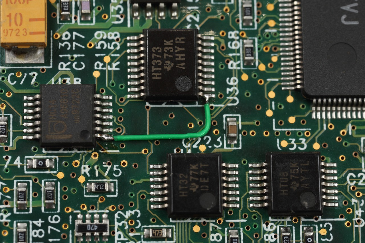
Hybrid designs – PCBs containing surface-mount (SMT) and through-hole (THT) parts – can be more expensive to assemble because they require different assembly processes. Therefore, avoid hybrid designs in favor of SMT-only PCBs. However, SMD and THT parts should be separated by side. In designs with THT parts at the top and SMT on both sides, manufacturers may charge extra for adding epoxy to the bottom parts during assembly.
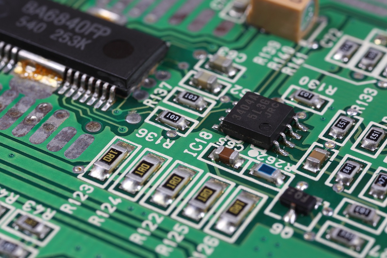
Annotate components with the appropriate silkscreen indicators, including the component type, a unique number, polarity indicators, and special pin markings. Doing so is recommended even if automated assembly is planned to facilitate post-production verification and troubleshooting. Designers should ensure that the text markings are placed in an unambiguous way, without overlaps, and in the same orientation as the part. Further, IC pin markings should be visible with the mounted chip in place.

DFM and Via Best Practices
Positions vias with sufficient clearance to nearby conductors, such as traces and other vias. Plated vias should have a hole diameter that follows at least a 1:1 ratio to the board’s substrate thickness, to ensure adequate copper build-up throughout the entire hole during fabrication. Plated vias will be narrower because of the additional plating.
The drill hole of vias may be slightly off-center. Thus, the annular ring should provide ample width to ensure that unplated via rings don’t lift during soldering or are susceptible to breaking during normal board operation because of the missing support from the plated barrel.
The clearance between exposed vias not adjacent to a connected pad and other conductors should be at least 0.15” to 0.2”. Generally, tented or plugged vias are preferred, especially in BGA designs with vias close to the BGA component’s solder pads. With other ICs, do not place vias under the chip unless done for thermal relief to prevent solder from wicking through the vias and remaining under the chip, potentially causing short circuits. Finally, via-in-pads should be copper-capped, and the opposite side should either be copper-capped or covered by a solder mask to make sure that plating chemicals don’t get trapped within the via.
Trace Routing Guidelines and Test Points
Teardrop pads can help prevent manufacturing problems at through-hole pads and when thin traces meet larger pads and vias. Trace necking is an approach that can help with soldering when applied to traces that are very long or connected to a large pad that would spread the heat too much and prevent adequate solder joint formation. Similarly, traces between adjacent components and pins should fan out instead of connecting the pads directly. This is done to prevent problems during soldering, such as tombstoning and cold solder joints.
Designers should add test points to critical nodes on the PCB and spread them around the entire board’s surface to make testing easier.

Component Placement Considerations for Solderability
Besides general PCB design best-practice approaches, like placing components sufficiently far apart to interfere with one another, designers should acknowledge the soldering process for optimized manufacturability. When wave soldering is employed, as usual with designs containing SMDs, designers should consider the board’s orientation when it travels through the molten solder. Typically, boards traverse the solder with their long side first to facilitate efficient soldering of components across the board’s width.
Place components so that larger parts do not shadow smaller devices. Further, components should be oriented on the board so that they travel through the solder wave in a way that ensures that the pins are soldered simultaneously. Additionally, similar components should be oriented the same way. Finally, designers should distribute devices on the entire board’s surface within reason to aid thermal balance and prevent warping during board assembly.
The Influence of PCB Classes on DFM
Board classes define the level of quality and reliability required for a particular application, and they typically range from class 1 to class 3, with class 3 being the highest. Class 1 boards are used in general consumer electronics, where functional performance is the primary concern and reliability is less critical. DFM for class 1 boards primarily aims to reduce cost, rather than to achieve stringent manufacturing requirements. In contrast, class 3 boards are designed for high-reliability applications such as aerospace, medical devices, or military equipment, where failure could bring severe consequences. DFM considerations for class 3 boards are the most stringent, ensuring the highest quality, reliability, and manufacturability.
Therefore, class 1 boards don’t require additional DFM measures or documentation unless desired. The board layout suffices and acts as the master drawing. However, designers may want to include supplementary notes for the board house.
Class 2 boards require a master drawing clearly describing the PCB’s physical dimensions, including the coating thickness and board plating. Additional QA test markings may be added, and pattern features, not referenced by hole size or location, need to be explicitly dimensioned through notes or referenced by a grid system.
Class 3 boards typically require more details and exact tolerance definitions, including board details, materials, detail markings, processing conditions, and design concepts. Board details include aspects such as type, size, shape, thickness, bow and twist (including tolerances), and stackup details. Materials include type, grade, color, and inks. Markings include safety markings, ESD details, and class regarding the voltage susceptibility. Processing conditions encompass the location of quality conformance coupons and definitions of the process specification and tolerances. The design concept outlines the location of test points, the grid system (metric or imperial), and a datum – a reference point on the PCB that allows machines to determine the board’s orientation.
PCB coupons are small PCB sections that are separate from the main assembly. They serve as sacrificial test pieces for quality assurance during manufacturing. These miniature samples let engineers test features like trace width, plating thickness, and solderability without risking the integrity of the main board. They are essential when conducting destructive tests. Each coupon has a unique identifier for easy tracking and correlating test results. Coupons are strategically placed on panels and adhere to different classes, depending on the intended tests.
Summary
DFM is a vital strategy for ensuring functionality, reliability, and cost-effectiveness during manufacturing. It involves understanding manufacturing processes, cost drivers, and best practices throughout the design process. PCB size, layer count, material choices, and component placement all impact manufacturing and assembly costs.
Due to different processes, hybrid designs containing SMT and THT components may have increased assembly costs. Proper component annotation and placement, including separation of SMD and THT parts and strategic fan-out of traces, are essential for efficient assembly and soldering.
Considerations for via placement, such as clearance to nearby conductors and proper annular ring width, ensure reliable connections and prevent manufacturing issues. Test point placement at critical nodes facilitates testing. Board classes define quality and reliability requirements for different applications, with Class 3 boards necessitating the most stringent DFM measures. PCB coupons serve as sacrificial test pieces and are vital for quality assurance during manufacturing, especially in domains that dictate high reliability and safety standards.


