


Understanding Blind and Buried Vias

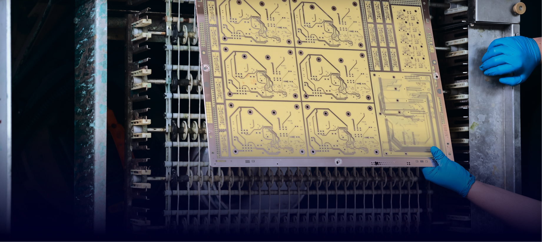
A topic that often comes up when discussing printed circuit board manufacturing is blind and buried vias. Here we’ll discuss what these are and how they can help you receive PCBs that function the way you intend. We’ll review the benefits of blind and buried vias, how they’re built, and why it’s vital to work with an experienced PCB manufacturer that knows how to properly add blind and buried vias to printed circuit boards.
It can often be difficult to fit all the needed connections on a PCB onto a single layer. A way around this problem is with vias. They are conductive holes that are shaped similar to a barrel, which allows for connections across multiple layers of the PCB. While there are several vias, there are two that are used most often. These are the blind and buried vias, and we believe they can provide some excellent benefits to those who use them in their PCBs.
What is the Difference Between Blind and Buried Vias?
A blind via will connect an outer layer of the board to one of the inner layers. However, it does not go all the way through the entire PCB. A buried via is located within the board and will connect the inner layers without reaching the outer layers. There is also a through-hole, which goes through the entire board vertically and will connect all the layers. It is a relatively simple concept to understand, and it can provide some excellent benefits.
Many Benefits of Blind and Buried Vias
Many PCB boards are small and have a limited amount of space, so the blind and buried vias can provide additional room and options for the board. The buried vias, for example, will help to free up space on the surface of the board without affecting the surface components or traces that are on the top or bottom layers. The blind vias can help to free up some additional space. They are often used for fine pitch BGA components. Since the blind vias only go through a portion of the board, it also means that there will be a reduction of signal stubs.
While the blind and buried vias can be used with many various PCBs, they tend to be used most often for high-density interconnect PCBs, or HDIs. The HDIs are popular because they can offer better power delivery and an added layer density. Through the use of the hidden vias, it will also help to keep the board smaller and lighter, which is very helpful when you are creating electronics. They are commonly used in medical devices, tablets, laptops, cellphones, and similar small electronics.
While the blind and buried vias can be helpful for those who need them, they can also add to the cost of the PCB. This is due to the added work that is required to add them to the board, along with the testing and manufacturing that will need to go into them. This means that you should only use them when it is truly necessary; because you want to have a great board that is tight and efficient.
How Are the Blind and Buried Vias Built?
The vias can be made either before or after the multilayer lamination. The blind and buried vias are added to the PCB through drilling, which can be precarious. It is important that the builder understands and is aware of the depth of the drill. If the hole is not deep enough, it might not provide a good connection. On the other hand, if the hole is too deep, there is a chance that it could degrade the signal or cause distortion. If any of these things were to occur, it would not be viable.
In a blind via, the hole will need to be defined using a separate drill file. The ratio of that hole diameter to the drill diameter needs to be equal to one or less. With a smaller hole, the distance between the outer layers and the inner layers will be smaller.
With a buried via, each of the holes needs to be made using a separate drill file. This is because they connect to different parts of the inner layer of the boards. The hole depth to drill diameter ratio will need to be no larger than 12. If it is larger than that, it will run the risk of touching other connections within the board.
We recommend working with AdvancedPCB for PCB manufacturing. This will help to ensure that the design and the build of the board, including the blind and buried vias, are feasible. Failure to prepare and to work with a quality board manufacturer could end up in added costs.
Our experts have the tools and techniques to ensure proper drill depths. We can ensure that there is no air trapped in the PCB during the process. The plating will be applied properly to connect the internal layers.
Choosing a Printed Circuit Board Manufacturer
Because it is so important to ensure blind and buried vias are added to the PCB properly, finding the right manufacturer becomes essential. We at AdvancedPCB provide reliable PCB manufacturing and assembly that meets your specifications.
We own a large printed circuit board manufacturing facility that uses state-of-the-art equipment and procedures to provide quality and consistency. All orders placed with us go through a free engineering file review before they go into production. This helps to ensure that the boards are created properly and that they work. No one wants to receive boards that are unusable. It would be a waste of time and money.
Also, we know how important it is for you to get your boards on time. We can provide you with PCBs with blind and buried vias with fast turnaround time, not to mention fast shipping.
When you are choosing a manufacturer, you will also want to have an understanding of how much the order will cost. We offer instant PCB quotes.
If you need PCBs that have blind and buried vias, the right company can make getting what you need fast and easy. AdvancedPCB offers excellent manufacturing, reliable products, and superior customer service.

AdvancedPCB
Related Posts
Vias, Sequential Lamination, and Plating: Navigating Their Role in Signal Integrity for PCB Design

Future trends of the circuit board
