Blog
Vias, Sequential Lamination, and Plating: Navigating Their Role in Signal Integrity for PCB Design
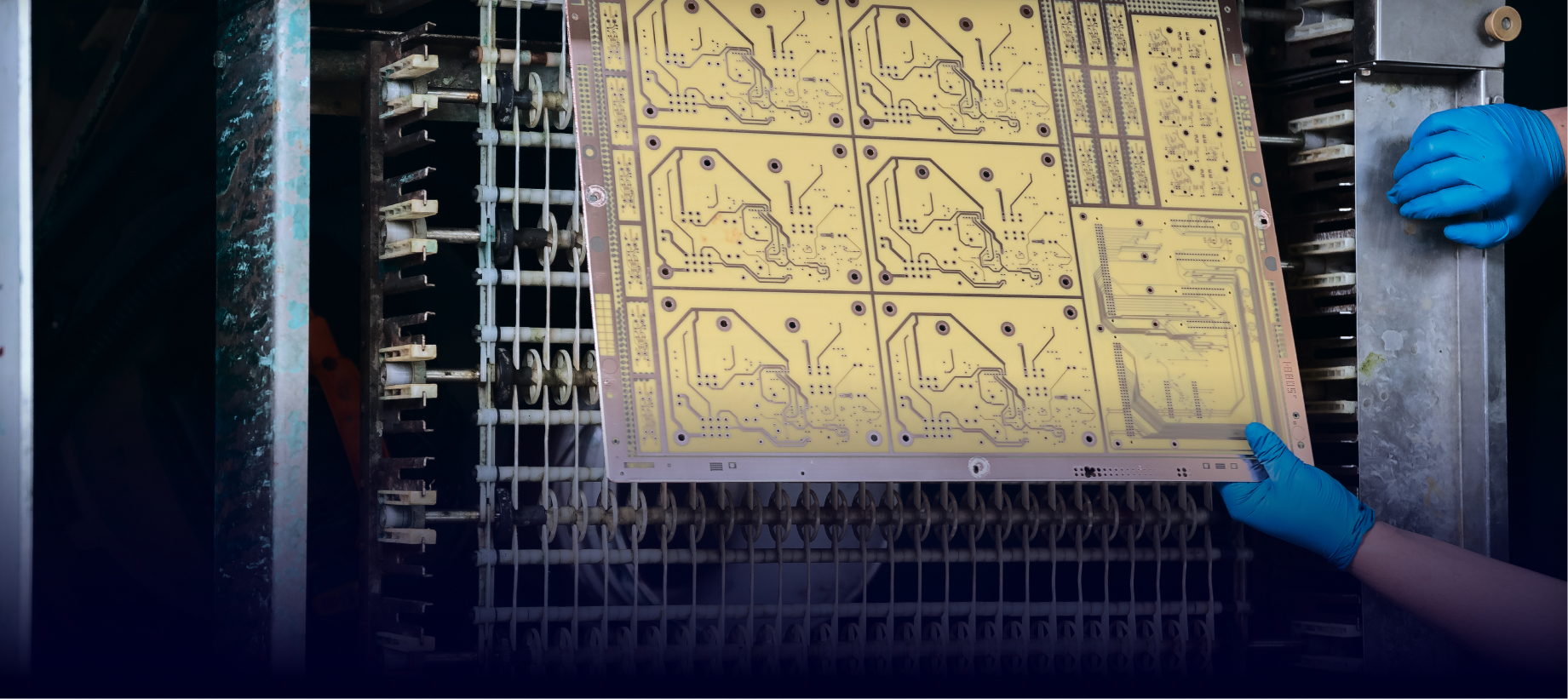
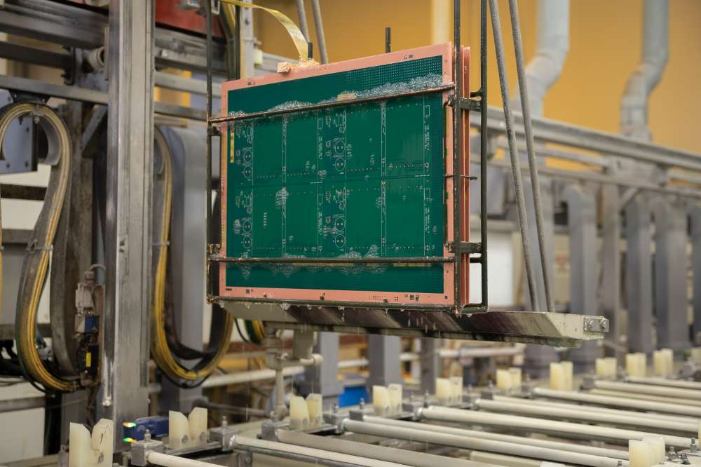
Welcome to the fascinating world of PCB design, where the interplay of various elements shapes the heart of modern electronics. Today, let’s have a chat about something crucial but often underrated – the impact of vias, sequential lamination, and plating on signal integrity.
Vias, Sequential Lamination, and Plating: Navigating Their Role in Signal Integrity for PCB Design
Read More
Editor's Picks
Vias, Sequential Lamination, and Plating: Navigating Their Role in Signal Integrity for PCB Design
Welcome to the fascinating world of PCB design, where the interplay of various elements shapes the heart of modern electronics. Today, let’s have a chat about something crucial but often underrated – the impact of vias, sequential lamination, and plating on signal integrity.
Vias, Sequential Lamination, and Plating: Navigating Their Role in Signal Integrity for PCB Design
Read More

Bridging the Gap: Why Designer-Fabricator Collaboration Matters in PCB Manufacturing
The relationship between designers and fabricators plays a crucial role in the success of any project. However, there has been an ongoing discussion about the disconnect between these two groups and the benefits of having designers who understand the intricacies of fabrication facilities.
Bridging the Gap: Why Designer-Fabricator Collaboration Matters in PCB Manufacturing
Read More

Navigating the Ever-Changing World of PCB Manufacturing: What Designers and Engineers Need to Know
In the world of Printed Circuit Board (PCB) manufacturing, the landscape is constantly evolving. With applications spanning across various industries, including Medical, Aerospace, Military, and more, designers and design engineers need to stay ahead of the curve.
Navigating the Ever-Changing World of PCB Manufacturing: What Designers and Engineers Need to Know
Read More
View All

Welcome Tom Caldwell, AdvancedPCB's New Chief Financial Officer

Welcome Gregory Halvorson, AdvancedPCB’s New CEO
.PNG?resizemode=force&maxsidesize=1226)
Choosing the Right Laminate Material for Your PCB Design
While PCB design has relied largely on the tried-and-true FR-4 substrate, many designs require more robust temperature or frequency performance to ensure their circuit performs optimally.
Choosing the Right Laminate Material for Your PCB Design
Read More

Questions from the Web
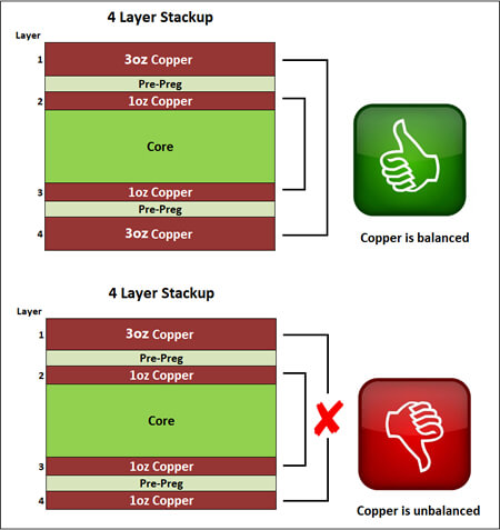
I have a question about the manufacturing capability for copper weights. Is it possible to use different copper weights on the same PCB?
Questions from the Web
Read More
The Importance of Power and Ground Planes in PCB Design
Ground and power planes are large conductive areas in a PCB design that serve diverse purposes. Ground planes provide a common reference point for electrical signals and serve as return paths for currents.
The Importance of Power and Ground Planes in PCB Design
Read More
Advanced PCB Routing Strategies
PCB routing is pivotal in ensuring the functionality, signal integrity, manufacturability, and reliability of electronic designs. Conductive traces are more than mere component interconnections or power distribution paths, and through effective routing, engineers can minimize signal degradation, crosstalk, and electromagnetic interference (EMI).
Advanced PCB Routing Strategies
Read More
Meeting the Moment: Filling the Jobs in the Semiconductor Industry
The Semiconductor Industry Association, the foremost trade group in the space, projected that 67,000 of the new jobs the CHIPS Act will create are vulnerable to vacancy in 2030.
Meeting the Moment: Filling the Jobs in the Semiconductor Industry
Read More
.png?resizemode=force&maxsidesize=1226)
Approaches to PCB Design for Signal Integrity and Manufacturability
fter formalizing a circuit’s functionality in a schematic diagram and deciding on the parts, devices, and technologies to employ, the next step is to create a functional PCB layout. This step aims to place all components on the PCB and establish all necessary connections, ensuring that the board dimensions are minimal and that application-specific goals, such as minimal losses or maximal signal integrity, are met.
Approaches to PCB Design for Signal Integrity and Manufacturability
Read More
Browse
All Categories